EMI Shielding Case ( An electromagnetic wave cover shades on PCB board)
Nowadays electronic products move towards multi-direction and multi-purpose conformity application. Technical product also creates more strict electromagnetic wave camouflage request day by day. Therefore, the effect of camouflage and application material of EMI (Electromagnetic Interference) become the most prior consideration for all the engineers of PDA、PDA Phone、Smart Phone、GPS and correlation product.
The EMI camouflage cover, may prevent the sensitive components from EMI disturbance excessively and avoid the other sensitive equipment to be disturbed by EMI.
By using characteristic of the EMI Shielding Case such as electric conduction, glitch and adumbrate may block or insulate spilling of electromagnetic wave efficiently. At the Same time it may help to reach the standard of safety examination. The effects (including interfering surrounded devices and affect human body) from electromagnetic wave of electronic products is one of the top consideration for all designer.
EMI Shielding Design
Nowadays the industry has noted demand of the CE/EMC, but along with the more electronic component use, compatibility of the electromagnetic wave also receiving same level of attention. Emission and tolerance of the electromagnetic wave should namely give the consideration at the beginning of the product design. But because of demanding of performance of the product often causes EMI problem to be unable to be adopted in the electronic component and fail to solve. Therefore, vessel and wire of the product should perform to camouflage (SHIELDING) to conform to the electromagnetic wave compatibility (EMC) to fit into all kind of standard.
EMI Shielding Serviceability
To conform to the EMC standard effectively, EMI Shielding is the only solution. It does not have to go through the long research and development and the test time, EMI Shielding will be the most cost benefit method to achieve EMC. The EMI Shielding not only suits of production of small and large size also for the products that involve high electromagnetism emission or the high electromagnetism sensitivity.
Emission and conduction of the electromagnetic wave
The electromagnetic wave appear in two kind of form, emission and conductivity. When its frequency is 10MHz or under mostly in conductivity, higher frequency are many form in emission. In order to prevent the electromagnetic wave to be spilled and interfered, case and cable of the product should be covered by high electromagnetism conduction material. A low frequency electromagnetic wave must with a thicker case, but relative may use a thinner surfaceto a high frequency electromagnetic wave.
Prevent electromagnetic wave penetration
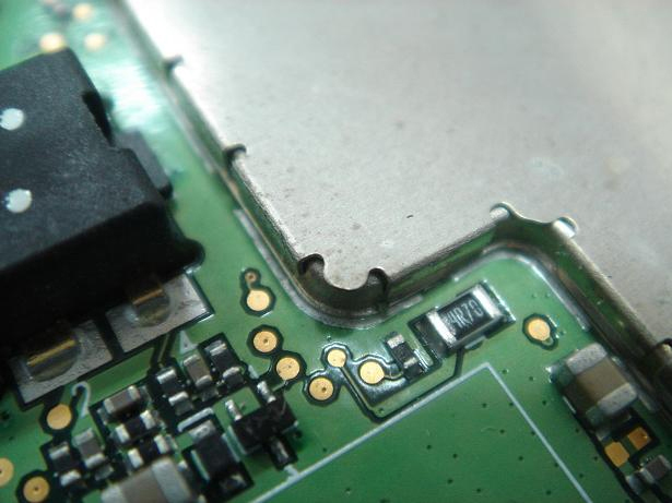
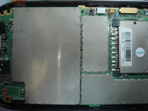
Higher frequency electromagnetic wave has shorter wave. In another words, along with the Electromagnetic wave frequency increase, it has higher capability to pass through smaller slit. Can of any electronic products should be a good electromagnetism wave resistance. An Ideal case of electromagnetism wave resistance should be no slit but an excellent conductor (metal ormetal superposition). Because cost, application, production and maintenance of product are considered, existing shielding can often has slit, gap, radiation hole, import and export wire andusing nonmetallic material. Therefore, to prevent electromagnetic wave pass through or spill out by using metal or metal superposition case and putting on the exterior wire, opens, gap of can aLabel EMI seal or pad will be the most efficient solution of electromagnetism wave resistance.
What is EMI(Electro-Magnetic Interference)?
Nowadays we take advantage of the infinite conveniences of all kinds of electronic system products 3C equipment, but also creates the complex electromagnetic wave environment. It’s so-called electromagnetic interfere (EMI),also called “the electronic noise”. Electromagnetic wave is electric wave and magnetic wave. In brief, it means the mobile electric current that exists inside of the electric wire. Its periphery undulation produces both electric field andmagnetic field. its frequency appears approximately in106 ~ 109 to Hertz. The common electric appliance produces wave frequency range as follows:
| Product |
Wave range MHz |
Product |
Wave range MHz |
Camcorder |
6 |
Vacuum |
200 |
TV |
20 |
Telephone
|
200 |
Laundry |
30 |
Computer
|
300~450 |
Hairdryer |
70 |
Cellular phone
|
700~1900 |
Coreless phone
|
250~380 |
Microware
|
2500 |
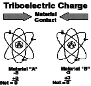
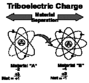
What is ESD(Electrostatic Discharge)?
Static is produced from electricity electric discharge. The simplest principle is after two matter contact and friction, anion of electricity ion from material surface, shifts to another material surface causes two substances to produce the electrostatic discharge.
What are the solutions applied for ESD and EMI on the industry, as well as their good
and bad in comparison. Some method has been utilized massively in our industry as
followed:
|
Method |
Good and Bad |
Adopted rate |
Solution 1 |
Change layout, adds on
ESD protector into
original IC design |
1.Time-consuming, must change the
design
2.Besides increase difficulty of the
design, it still needs the attention to
the extra cost which ESD protector
circuit increases. For example the
layout area increases or extra cost on
adding manufacture step |
10% |
Solution 2 |
Addsanelectricconduction paint (picture 1) |
1. High cost
2 .Time-consuming |
10% |
Solution 3 |
Has not done specially measure |
Although when the mobile phone has big volume, problem not easily to be Discovered. But this is extremely Irresponsible procedure. Especially, nowadays in European and American countries more and more take EMI may caused injury to human body seriously.
This kind of design can directly affect sale volume to these nations |
10% |
Solution 4 |
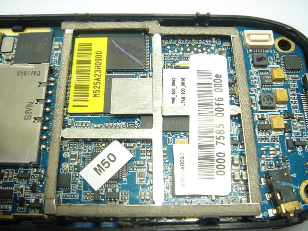
ESD/EMI can (Picture 2)
uses cover and base design
|
It is half of thermal paste in cost |
70% |
New patent design |
Case, Support plate integrate into PCBA |
Cost is estimated to be 1/3 cheaper then solution 4 |
0% |
Attached figure one
Attached figure one